A snubber circuit, also known as a snubber network or snubber damping circuit, is an electrical circuit used to protect electronic components from voltage spikes or transient overvoltages. It is typically employed in power electronics applications, such as power supplies, motor drives, or switching circuits, to mitigate the effects of rapid voltage and current changes.
The primary purpose of a snubber circuit is to suppress voltage or current transients that can occur when switching an inductive load, such as a relay or a transformer. These transients are caused by the energy stored in the inductive component, which can lead to voltage spikes or ringing phenomena. Snubber circuits are designed to absorb this excess energy and provide a controlled discharge path for it.
When an inductive or capacitive load is switched on or off in a circuit, voltage and current transients can be generated due to the sudden change in energy flow. These transients can cause problems such as voltage spikes, ringing, or electromagnetic interference (EMI). A snubber circuit helps mitigate these issues by providing a path for the energy to dissipate and dampening the transients.
A snubber circuit usually consists of passive components, such as resistors, capacitors, and sometimes diodes. The most common types of snubber circuits are RC snubbers and RCD snubbers:
RC Snubber:
This type of snubber circuit includes a resistor (R) and a capacitor (C) connected in series or parallel across the switch or component being protected. The resistor dissipates energy and limits the rate of voltage change, while the capacitor absorbs and stores the excess energy, reducing the voltage spike.

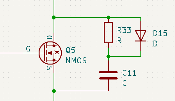
RCD Snubber:
In an RCD snubber circuit, a resistor (R), a capacitor (C), and a diode (D) are connected together. The resistor and capacitor perform similar functions as in the RC snubber, while the diode provides a discharge path for the stored energy when the voltage across the component reverses.
R-C Snuber Demonstration as follows refer the more info the following Link


Calculate the R-C Snuber (Ref site Link
 a
aBy properly selecting the values of the components in a snubber circuit, the voltage spikes and transients can be significantly reduced, protecting sensitive components from damage and improving overall system performance. The design of a snubber circuit depends on various factors, including the load characteristics, switching frequency, and required level of protection.
It's important to note that snubber circuits are application-specific, and their design should consider the specific requirements and parameters of the system being protected. Therefore, careful analysis and consideration of the circuit's behavior are necessary to ensure effective snubber operation.
No comments:
Post a Comment